
The Threat of In-House Chips: Deep Dive on Google TPU v7 vs. Amazon Trainium 3
The AI hardware landscape in 2026 is defined not just by traditional semiconductor vendors, but increasingly by hyperscalers building their own, deeply integrated silicon. Among the most important examples are Google’s TPU v7 and Amazon’s Trainium 3, two generations of in‑house accelerators aimed squarely at large‑scale AI training and inference in their respective clouds.

In‑house AI accelerators like TPU v7 and Trainium 3 are not merely alternative compute options; they are strategic levers. They shape cost structures, influence developer ecosystems, and can tilt the economics of AI workloads in favor of the clouds that own them. Understanding the “threat” they pose involves looking at their technical roles, their integration into cloud platforms, and the broader consequences for the AI hardware market.
Why in‑house chips are strategically threatening
To grasp the threat posed by TPU v7 and Trainium 3, it helps to see why hyperscalers build in‑house chips at all. The core motivations are cost control, differentiation, and architectural freedom.
Cost control is straightforward: when a cloud provider can design chips tailored to its workloads and purchase them at internal transfer‑pricing rather than market rates, it can reduce the per‑unit cost of compute. Over time, this can translate into more competitive pricing or higher margins on AI services.
Differentiation matters because in‑house silicon can expose capabilities unavailable on third‑party hardware. Specialized tensor units, custom dataflow architectures, and deep integration with proprietary software stacks allow clouds to offer unique performance, features, or service tiers that are hard to replicate elsewhere.
Architectural freedom allows hyperscalers to co‑design chips with networks, storage, and orchestration layers. They are not bound by the constraints of merchant product roadmaps and can prioritize the features that align most closely with their long‑term strategies.
In combination, these factors make in‑house chips a threat: they can erode demand for general‑purpose GPUs in certain workloads, lock customers into proprietary ecosystems, and shift bargaining power in favor of clouds rather than traditional chip vendors.
Google TPU v7: evolution of a dedicated AI fabric

Google’s TPU family has long focused on providing a dedicated, high‑efficiency platform for deep learning workloads. By the time TPU v7 arrives, several design themes are well established: systolic arrays for matrix multiplication, tight integration with Google’s networking and storage fabric, and deep coupling with framework support centered around TensorFlow and other internal tools.
TPU v7 can be seen as an evolution of this design philosophy. Its architecture is tuned for large‑scale training of frontier models as well as high‑throughput inference for Google’s own services and cloud customers. The core compute fabric is built around dense matrix units, supported by high‑bandwidth memory and interconnects optimized for dataflow‑style workloads.
Crucially, TPU v7 is not a standalone chip; it sits inside carefully designed pods and clusters. Google’s internal software stack understands TPU topology, scheduling workloads to minimize communication overhead and maximize utilization. This combination of hardware and orchestration makes TPU v7 a cornerstone of Google’s AI infrastructure rather than just another accelerator SKU.
From the outside, TPU v7 thus represents both a technical achievement and a strategic asset: it allows Google to run its own large‑scale models and offer training services at performance and cost profiles that reflect years of co‑design.
Amazon Trainium 3: extending a heterogeneous cloud strategy
Amazon’s Trainium line fits into a broader strategy of offering a heterogeneous set of accelerators in AWS: from GPUs to in‑house chips like Trainium for training and Inferentia for inference. Trainium 3 continues this trajectory, focusing on providing high‑performance training silicon deeply integrated into AWS services.
Trainium 3 is architected to serve a wide range of training workloads on AWS, including language models, vision systems, and recommendation engines. Like TPU v7, it emphasizes efficient matrix and tensor compute, leveraging specialized units and memory architectures tuned for popular model types.
Where Trainium 3 differs is in its integration story. It is designed to slot seamlessly into AWS’s existing stack: EC2 instance families, managed services like SageMaker, and storage and networking fabrics tuned for cloud‑native workloads. Tooling supports mainstream frameworks, and AWS makes concerted efforts to simplify porting and optimization, so customers treating Trainium as “just another instance type” can adopt it without rewriting everything from scratch.
Trainium 3, therefore, is part of a broader pattern: AWS building custom hardware to anchor specialized instance families and services, reinforcing its ability to shape price‑performance curves for AI workloads independent of third‑party chip vendor decisions.
Technical themes: what TPU v7 and Trainium 3 aim to optimize

Even without focusing on exact specifications, several common technical themes define what TPU v7 and Trainium 3 aim to optimize.
First, both target high throughput for dense linear algebra kernels—the backbone of deep learning. Their compute units are designed around matrix and tensor operations, with dataflow or systolic execution models that keep arithmetic units busy while minimizing control overhead.
Second, memory and interconnect architectures are tuned for AI workloads. High‑bandwidth memory interfaces feed compute units, while interconnects support fast communication within nodes and across multi‑chip systems. Both chips are meant to scale out into clusters that can handle very large models and batch sizes.
Third, energy efficiency is a critical goal. In‑house chips must deliver substantial performance per watt to justify their existence relative to merchant alternatives. TPU v7 and Trainium 3 are therefore designed with power‑aware data paths, optimized voltage and frequency domains, and runtime management that keeps energy budgets in check while training and inference jobs run.
Together, these themes reflect a focus on making custom silicon that is not only powerful but also tightly aligned with the cost and capacity realities of hyperscale data centers.
Integration into cloud services: where the threat multiplies
The true threat of in‑house chips like TPU v7 and Trainium 3 emerges when they are integrated into cloud services, not just exposed as bare metal or instance types.
Google wraps TPUs in managed services: training platforms, inference endpoints, and specialized pipelines for its own products. Cloud customers can access TPUs through high‑level APIs and managed offerings, often without dealing directly with hardware details. This shifts competition from “chip versus chip” to “end‑to‑end service versus service,” where Google’s TPU‑based stack may offer distinct performance or cost advantages.
AWS follows a similar path. Trainium 3 appears in specific instance families and integrates with services like SageMaker, enabling customers to train models with minimal setup while benefiting from underlying hardware optimization. AWS can tailor pricing, capacity allocation, and instance placement to make Trainium 3 attractive for certain workloads.
In both cases, integration multiplies the effect of the chips themselves. Rather than competing only at the hardware level, in‑house accelerators compete as part of full AI platforms, which is where their threat to merchant vendors truly crystallizes.
Developer experience: frameworks, tooling, and lock‑in dynamics

From a developer perspective, the value and risk of in‑house chips is mediated by frameworks and tooling. TPU v7 and Trainium 3 are only useful to the extent that developers can target them comfortably.
Google leans on TensorFlow and other internal frameworks, offering optimized paths for TPU workloads. Model authors can use familiar abstractions, with back‑ends that map computational graphs onto TPUs efficiently. However, this pairing also deepens the TPU‑TensorFlow link, potentially nudging developers toward parts of the Google ecosystem.
AWS aims to support popular frameworks like PyTorch and TensorFlow, providing tooling to compile and optimize models for Trainium 3. The more friction AWS removes in targeting Trainium, the more likely customers are to adopt it for production workloads, reinforcing AWS’s position as a full‑stack AI platform.
Lock‑in dynamics arise because optimized models and pipelines may rely on vendor‑specific compilers, libraries, or instance types. Migrating from TPU‑based or Trainium‑based deployments to other hardware can involve non‑trivial work, giving hyperscalers an advantage in retaining customers once they adopt in‑house silicon deeply.
Economic implications: price‑performance and bargaining power
Economically, TPU v7 and Trainium 3 influence two major variables: price‑performance ratios for AI workloads and bargaining power in the hardware supply chain.
On the price‑performance side, in‑house chips allow hyperscalers to craft tailored pricing schemes. They can pass some of their internal silicon cost savings to customers in the form of lower per‑unit compute prices or more favorable quotas, especially for training. This can pressure competitors relying heavily on merchant GPUs to match pricing or differentiate in other ways.
In terms of bargaining power, building in‑house chips gives hyperscalers leverage in negotiations with external vendors. They can compare internal options against merchant offerings, potentially demanding better terms from GPU providers or limiting reliance on external supply during periods of scarcity. This changes the dynamics of the AI chip market, where large cloud platforms become both customers and competitors to traditional semiconductor firms.
These economic shifts underscore why in‑house chips are perceived as a threat: they alter the balance of power in the AI hardware ecosystem, with hyperscalers gaining more control over key cost and capacity levers.
Impact on merchant GPU vendors and other accelerator providers
For merchant GPU and accelerator vendors, the rise of TPU v7 and Trainium 3 means that some portion of cloud demand is now redirected away from their products. Even if hyperscalers continue to buy GPUs at large scale, every in‑house chip that occupies a slot in a rack represents a non‑sale for external suppliers.
Moreover, in‑house chips set new benchmarks that merchant vendors must respond to. If TPU v7 or Trainium 3 achieve compelling performance or efficiency for certain workloads, GPUs and other accelerators must match or exceed those benchmarks to stay attractive. This can accelerate innovation but also compress margins as competition intensifies.
Merchant vendors may respond by strengthening their own software ecosystems, emphasizing flexibility across clouds, and building closer partnerships with enterprises that prefer multi‑cloud or on‑prem deployments not tied to a single hyperscaler’s silicon. They may also pursue semi‑custom collaborations with clouds that do not build their own chips.
In any case, the strategic threat is clear: in‑house accelerators reduce addressable market segments and raise the bar for performance and integration that merchant vendors must meet.
Customer perspective: choice, flexibility, and risk
From a customer standpoint, the availability of TPU v7 and Trainium 3 is both an opportunity and a risk. On one hand, these chips can offer excellent performance and cost for workloads that match their strengths. On the other hand, deep reliance on vendor‑specific hardware can reduce flexibility.
Customers adopting TPU‑ or Trainium‑centric architectures must consider how easily they can migrate workloads if business or regulatory needs change. They must assess whether optimized models and pipelines can be ported to other hardware without significant rework, and how cloud‑specific AI services fit into broader multi‑cloud or hybrid strategies.
Some organizations may embrace in‑house chips wholeheartedly, betting on deep integration with a single cloud. Others may hedge, mixing workloads across clouds and hardware types, or prioritizing portable frameworks and deployment models even if that means foregoing some optimization.
In this sense, the threat of in‑house chips is not only to hardware vendors but also to customer flexibility, making strategic planning around AI infrastructure more complex.
Future trajectories: convergence, competition, or coexistence?
Looking ahead, several trajectories are possible for the relationship between in‑house chips like TPU v7 and Trainium 3 and merchant accelerators.
One scenario is convergence, where standards and tooling evolve to make cross‑platform deployment smoother, reducing the practical lock‑in of custom silicon. In this world, TPU and Trainium coexist with GPUs, with customers choosing hardware based on workload fit while maintaining portability.
Another scenario is intensified competition, where clouds lean harder into proprietary chips and tightly integrated services, aiming to capture and retain customers inside their ecosystems. Merchant vendors respond by doubling down on open tooling and diverse deployment options, positioning their hardware as the backbone of multi‑cloud and on‑prem strategies.
A third scenario is coexistence with segmentation: in‑house chips dominate certain workload types and customer segments (e.g., large cloud‑native AI deployments), while GPUs and other accelerators remain primary choices for enterprises, research organizations, and hybrid environments where flexibility and existing investments matter more.
Whichever trajectory unfolds, the presence of TPU v7 and Trainium 3 ensures that AI hardware decisions will be more strategic, nuanced, and tightly linked to cloud platform choices than in earlier eras.
Conclusion: in‑house chips as a new center of gravity in AI hardware
The emergence of Google TPU v7 and Amazon Trainium 3 illustrates how in‑house chips have become a new center of gravity in AI hardware. They embody a shift from clouds as mere consumers of accelerators to clouds as designers and owners of critical silicon, reshaping cost structures, performance baselines, and ecosystem dynamics.
For traditional chip vendors, developers, and customers, this shift is a threat insofar as it concentrates power and innovation within a handful of platform providers. It is also an opportunity to rethink how AI hardware, software, and services interlock. As TPU v7 and Trainium 3 extend their reach across their respective clouds, understanding their role—and the broader implications of in‑house silicon—is essential for anyone navigating the future of AI infrastructure.
You May Like

Narrowing Spread Between NAND Spot and Contract Prices in 2026 – A Signal
By 2026, one of the most watched metrics in the NAND flash market has started to shift in a subtle but meaningful way: the spread between spot prices and long‑term contract prices is narrowing. For casual observers, this may look like just another incremental change in a notoriously volatile industry. For memory makers, module houses, device OEMs, and data center buyers, however, a tightening gap between spot and contract prices is a signal—a reflection of evolving supply–demand balance, risk perceptions, and strategic behavior on both sides of the market.

Price Divergence Trading Strategies Between NAND Flash and DRAM ETFs
NAND flash and DRAM sit at the core of AI storage and computing power. Both are memory, but they are not the same business. DRAM is main memory—fast, volatile, and central to high‑bandwidth workloads like AI training and inference. NAND is non‑volatile storage—slower than DRAM, but crucial to persistent data and large‑scale object storage. The cycles that drive their pricing and margins overlap, yet they often diverge. That divergence is where trading strategies between NAND and DRAM ETFs become interesting.

China’s HBM Localization Progress: The Catch-Up Pace of CXMT and XMC
China’s drive to localize advanced memory technologies has accelerated over the past several years. High-Bandwidth Memory (HBM) sits near the center of that strategy because it is integral to AI accelerators, high-performance computing (HPC) and other strategic compute platforms. Two domestic players—ChangXin Memory Technologies (CXMT) and XMC (Xianghui Memory, commonly referred to as XMC)—have become focal points in assessing how quickly China can close the gap with international incumbents on HBM die, stacking, and packaging.
Thermal Simulation Challenges and Solutions in 3DIC AI Chip Design
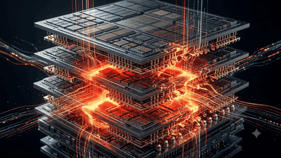
As AI workloads push chips to deliver ever higher compute density, designers are increasingly turning to three‑dimensional integration (3DIC) to stack dies vertically and pack more functionality into limited footprints. While 3DIC architectures unlock significant performance and bandwidth advantages, they also introduce complex thermal behaviors that are far harder to predict and manage than in traditional 2D layouts.
An Attempt at Compiling a Memory+Compute Fusion Thematic Index – A Dual-Track Framework
Most AI investors talk about “compute” as if it were the whole story: GPUs, accelerators, chips, cores. But every one of those cores needs somewhere to read from and write to. Memory and storage define how wide the data highway really is. In practice, AI performance is a fusion of compute and memory, not a solo act. So why do so many indices and ETFs separate them into different silos—one for semiconductors, one for memory, one for data centers—when the actual workloads keep blending them?

Surging Demand for Laser Drilling and Plasma Dicing Equipment in Advanced Packaging
Advanced packaging has become one of the semiconductor industry’s most important growth engines, and it is now pulling a surprising set of process tools into the spotlight. Among the most in-demand are laser drilling and plasma dicing equipment. These machines sit close to the heart of heterogeneous integration, fan-out packaging, wafer thinning, TSV formation, glass substrate processing, and other advanced flows where precision, yield, and throughput matter enormously. As packaging moves from a back-end afterthought to a strategic platform, the equipment used to shape, open, and separate materials has become just as important as the dies themselves.

D2D Interface Bandwidth and Latency Comparison in Chiplet Architectures
Chiplet architecture has turned the package into a real performance battleground. Once multiple dies are placed side by side or stacked within the same advanced package, the quality of the die-to-die, or D2D, interface becomes one of the most important determinants of system behavior. Bandwidth is no longer a nice-to-have metric, and latency is no longer a small implementation detail. Together, they shape whether a chiplet system feels nearly monolithic or frustratingly fragmented.

Stock Selection Logic and Alpha Validation of ESG-Themed Semi ETFs
Semiconductor themed ETFs are no longer just about growth and cycles. A growing subset now layers environmental, social, and governance (ESG) criteria on top of traditional sector exposure. These ESG semi ETFs promise two things at once: access to one of the market’s most powerful secular themes, and alignment with sustainability and governance standards. The pitch is appealing, but it raises two hard questions. First, how exactly are these stocks being selected? Second, does the ESG overlay help, hurt, or leave alpha unchanged?